In a previous article I introduced Ngspice as a popular open source circuit simulation tool. After some more time playing with circuits, I stumbled into KiCad, a popular open source tool for designing circuits.
KiCad focuses on design of schematics (diagrams that show components and how they are connected) and PCBs. On top of this, KiCad can integrate with Ngspice to run simulations on the schematics we design, making it an all-in-one tool for circuit design.
Installation
We can get the latest version of KiCad from their downloads page. Installing it in Ubuntu, is as easy as running these commands:
1
2
3
sudo add-apt-repository ppa:kicad/kicad-7.0-releases
sudo apt update
sudo apt install kicad
Creating a project
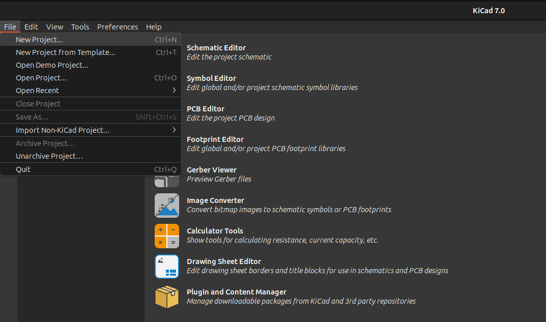
When we start KiCad we are going to be welcomed by the main KiCad window. From here, we want to start a new project. We can do this by clicking File -> New Project (Ctrl+N)
This will open a new window where we can choose a name for our project and a folder where we want to create it:
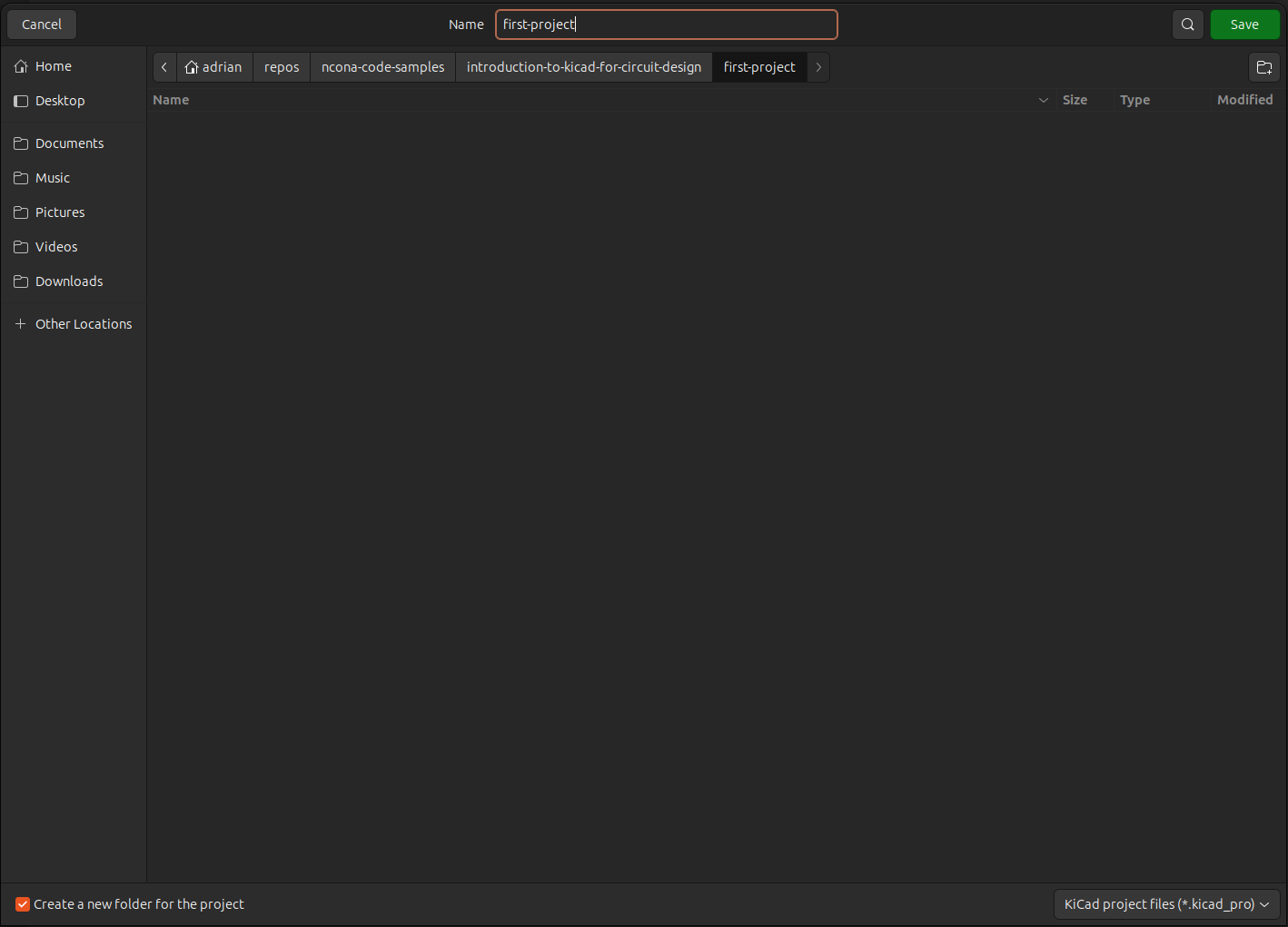
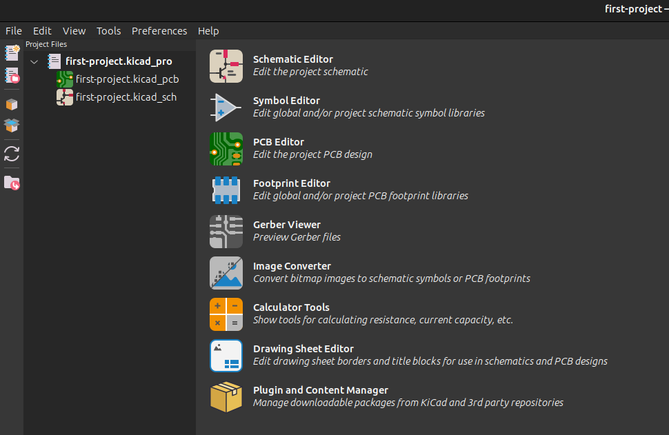
A new folder will be created with the same name as our project. The project files will be shown in the left part of the main window.
Designing a Schematic
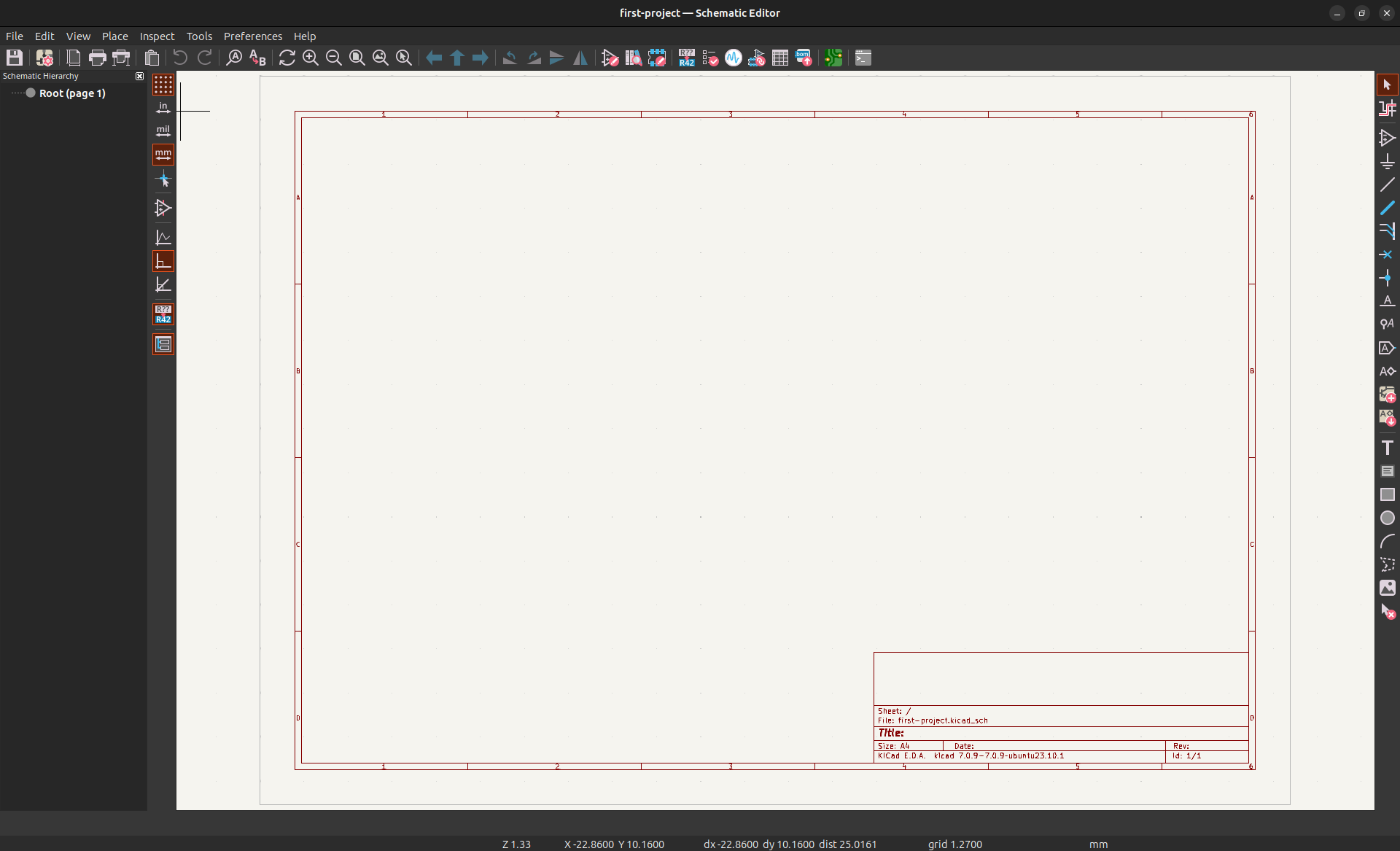
After creating our project, we want to start designing our circuit schematic. To get started, we need to click on the Schematic Editor icon on the right:
![]()
The Schematic Editor window will open:
In the bottom right corner of the sheet we can see some information about our schematic. Let’s give our schematic a title.
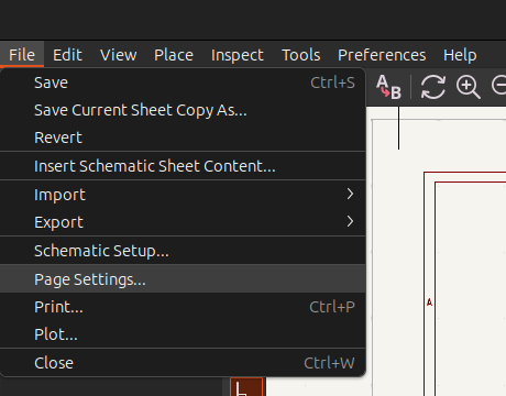
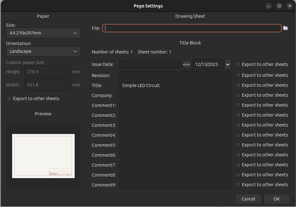
First of all, we need to go to Page Settings:
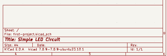
This will open a new window. Let’s set the title to Simple LED Circuit:
The title will be reflected in our schematic:
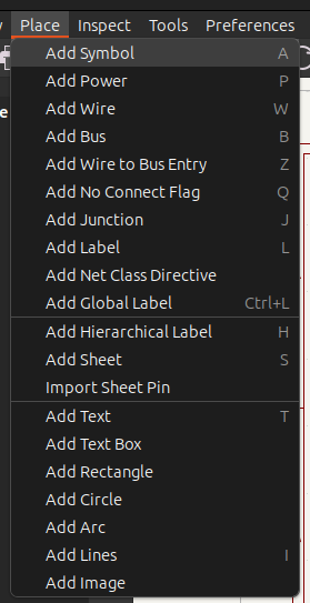
We can now add our first symbol. Open the symbol selection window by clicking Place -> Add Symbol (A):
Or by clicking the Add Symbol icon on the right toolbox:
![]()
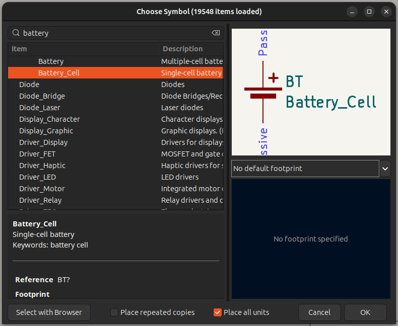
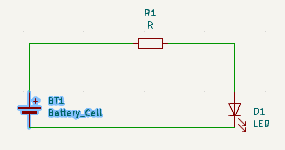
The Choose Symbol window allows us to browse the different symbols or to search for them. Our first symbol is going to be battery; For this, we’ll choose Battery_Cell:
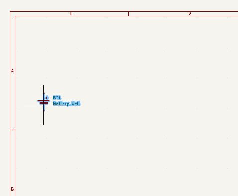
After clicking OK, we’ll see the symbol floating next to our cursor. We just need to click wherever we want to insert the symbol:
After inserting our symbol, we can hit the Esc key to go back to the default cursor.
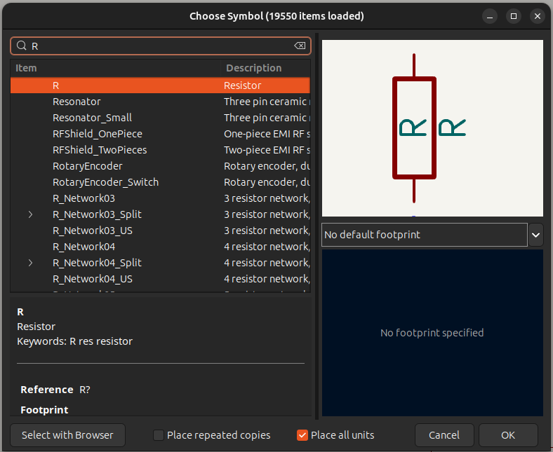
We’ll also need a resistor, so we can follow the same process. One thing to keep in mind is that in KiCad resistors are just called R:
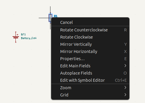
Resistors are by default inserted vertically. We can rotate our resistor by right clicking on it and choosing Rotate Counterclockwise (R):
Finally, we’ll insert an LED:
Before we continue to the next step, it’s probably a good time to talk about how we can move around a schematic.
To zoom into a specific part of our schematic we just need to point our cursor to the part we want to zoom in and scroll up with our mouse scroll wheel (If we are using a trackpad, we can swipe up with 2 fingers). To zoom out we just need to scroll down (swipe down).
To pan (move around the schematic), we just need to click and hold the scroll wheel and move the cursor in the direction we want to move.
With this information, we can zoom into our components to start the next step; Connecting our components.
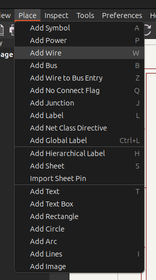
We can do this by choosing Place -> Add Wire (W), or clicking the wire icon on the toolbar on the right:
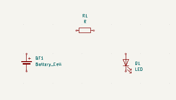
We can then proceed to click on the positive terminal of the battery, followed by the left terminal of the resistor and continue until the schematic looks like this:
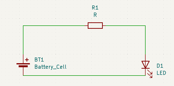
At this point, our simple schematic is complete.
SPICE Simulation
So far, our schema is just a drawing. To make sure it does what we want it to do, we need to convert it to a spice model and run a simulation.
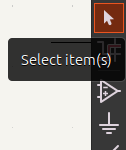
We’ll start by selecting our voltage source. To do this we need to choose the select tool on the toolbar (Esc):
With the select tool set, we need to click our voltage source and it will become highlighted:
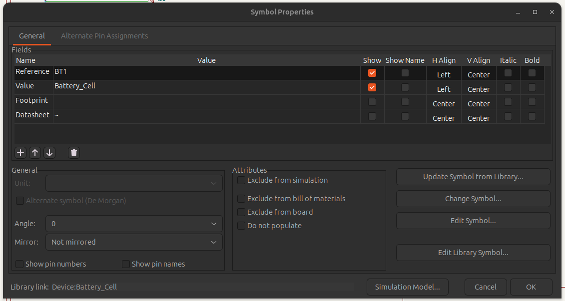
Use the e key to open the Symbol Properties window and click the Simulation Model... button (located at the bottom-right):
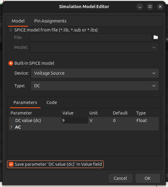
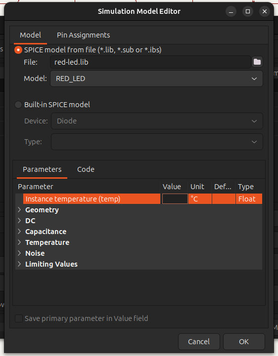
A new window titled Simulation Model Editor will open. Update the values to match the following picture: (The important values are: Voltage Source, DC and 9):
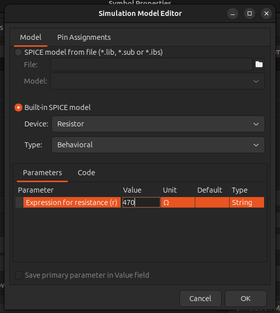
We are going to do the same for the resistor, but we’ll choose these values:
The LED is a little trickier, since KiCad doesn’t include a SPICE model for an LED. When we encounter this issue, our best bet is to search for the model on the internet. Ideally, we would find it at the manufacturer’s website, but sometimes it might be harder to find.
This is one of the models for an LED I found online:
1
.model RED_LED D (IS=93.2P RS=42M N=3.73 BV=4 IBV=10U CJO=2.97P VJ=.75 M=.333 TT=4.32U)
We want to create a file in our project folder named red-led.lib and add the above model as its content.
Once we created the model, we can associate that model in our diagram:
When using external models, it’s important to make sure that pins are correctly mapped to their function. To verify this, we can select the Show option for Sim.Pins.
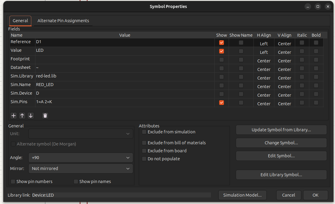
This will cause the pin mapping to be shown in the schematic:
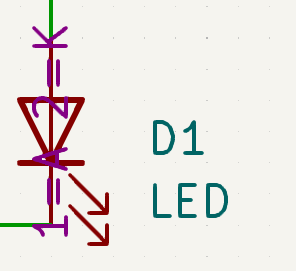
It’s not very easy to read, but we can see that it says 1 = A at the bottom and 2 = K at the top. This doesn’t match the diode icon, which has the anode at the top and cathode at the bottom. We need to fix this by updating Sim.Pins:
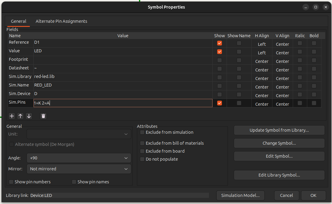
Now that our LED is correct, we can hide the Sim.Pins if we want to.
Spice requires us to define a reference to ground (voltage 0) in our diagram, so let’s take care of that. We can do it from Place -> Add Power (P):
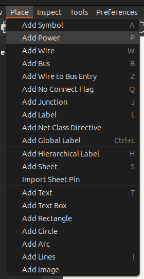
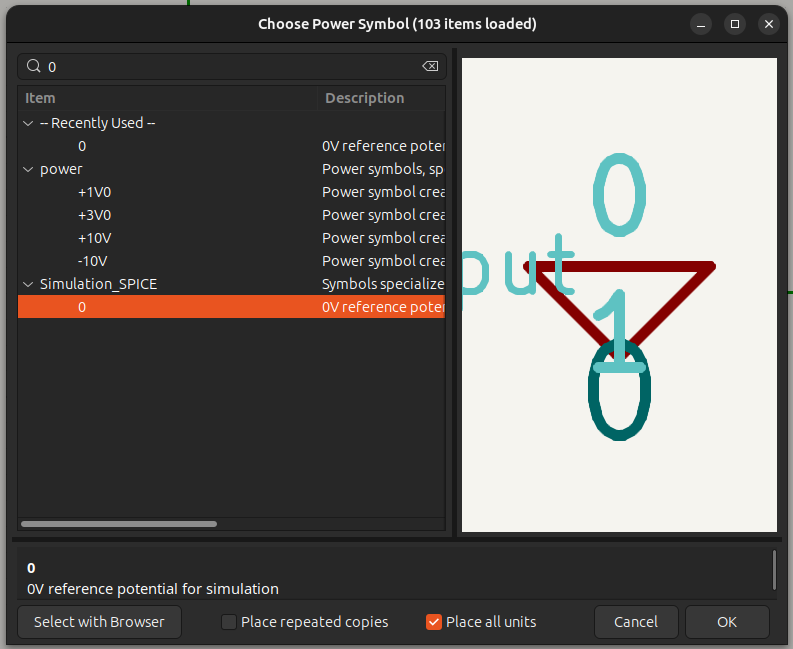
We will use the 0V reference symbol:
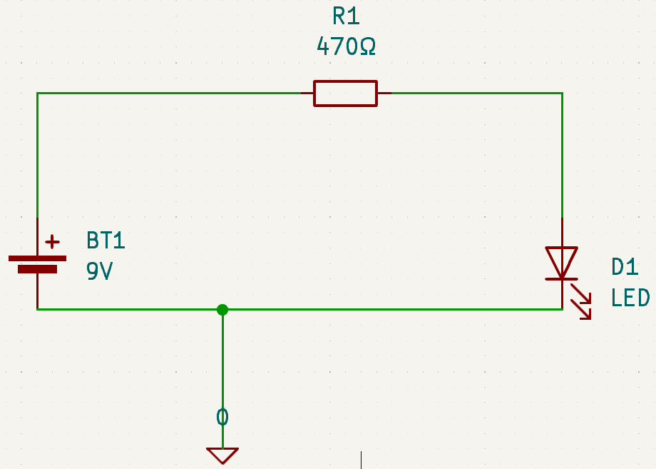
We’ll place it at the bottom of our diagram and connect it with a wire:
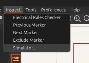
With all our components correctly modeled, we can go to Inspect -> Simulator:
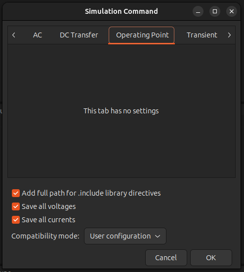
From the SPICE Simulator we’ll choose Simulation -> Settings. A window will pop-up. From there we navigate to the Operating Point tab and click OK:
This will enable the Run/Stop Simulation Button. Click the button and the results will be printed:
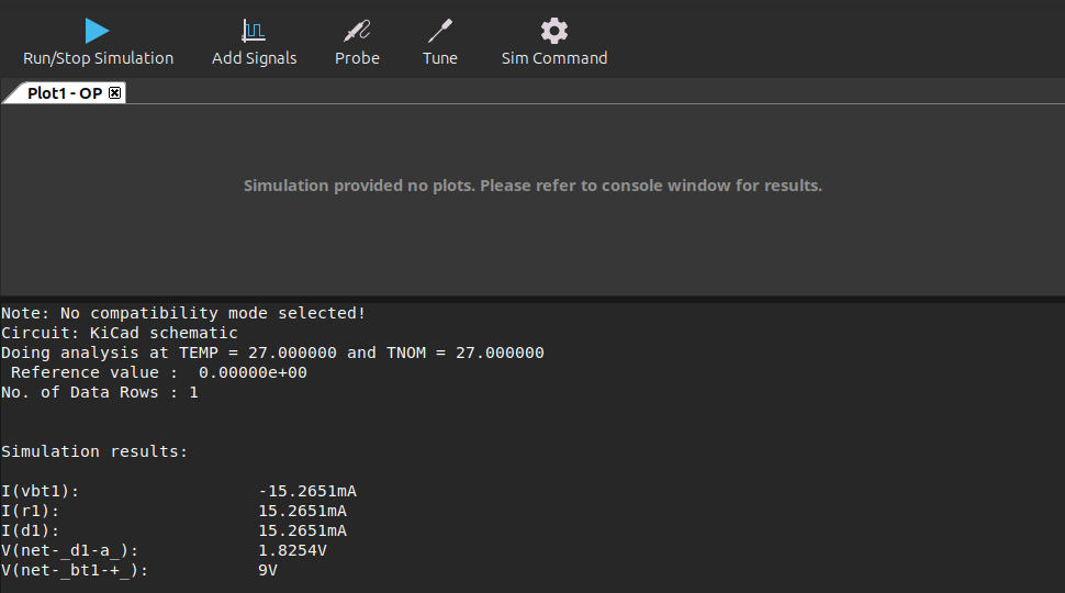
The results tell us that there are 15.26mA running through the circuit. It also tells us that the voltage at the positive pole of the battery is 9v and the voltage after the resistor is 1.82V.
You might be asking yourself where net-_d1-a_ and net-_bt1-+_ come from. These are the names of our nets (you can think of them as buses, connecting points, or cables). Since we didn’t assigned names to them, KiCad did it for us. We can change their names to make them more meaningful.
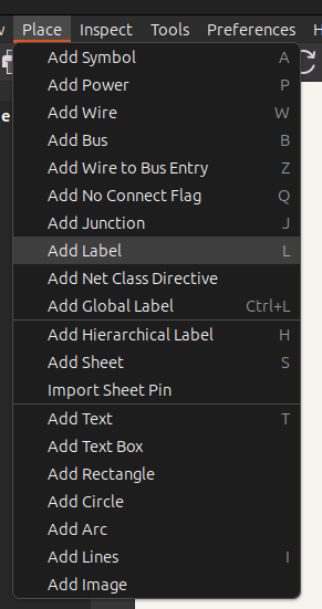
From the schematic editor, select Place -> Add Label (L):
Here we can input the name of our net. We’ll use Vin for the wire connecting our voltage source to the resistor:
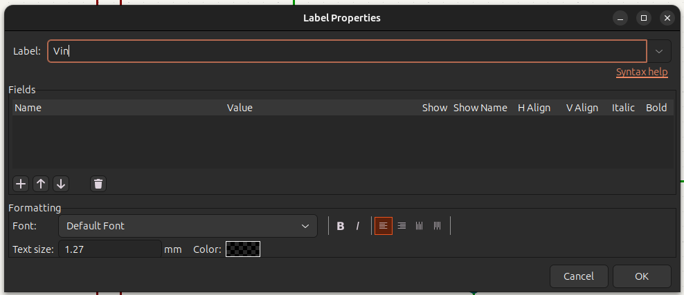
After clicking OK, we can click on the wire where we want to add that label. We’ll do the same for the Anode cable.
If we run our simulation again, our new labels will take effect:
1
2
3
4
5
6
7
Simulation results:

I(r1):                    15.2651mA
I(d1):                    15.2651mA
I(vbt1):                  -15.2651mA
V(/anode):                1.8254V
V(/vin):                  9V
Designing the PCB
Before we can start designing our PCB, we need to add footprints for our components. Footprints define the shape of a component in the PCB.
To define the footprint for our battery, we need to open the symbol properties for our voltage source, click on the empty box next to Footprint and click the library icon that appears next to it:
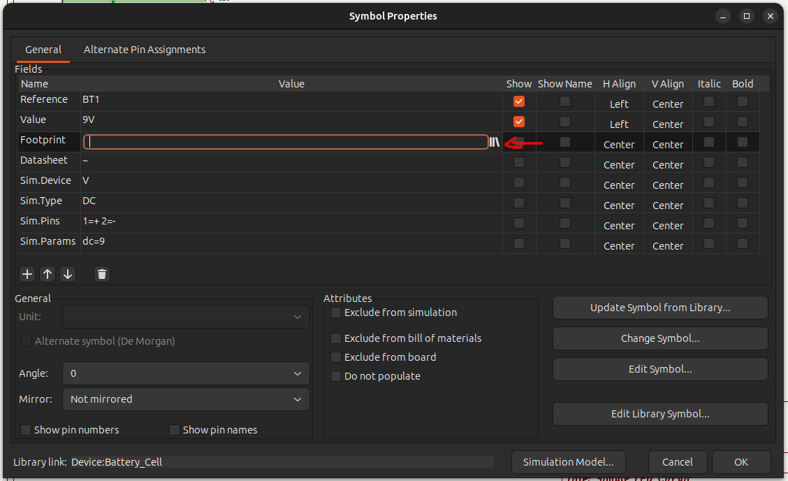
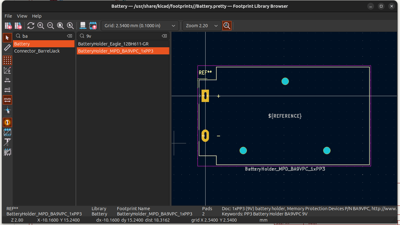
The footprint browser allows us to filter the components based on category and name. For our battery we will choose Battery:BatteryHolder_MPD_BA9VPC_1xPP3, which is a 9V battery holder:
For the resistor, I found this website that describes the different types of resistors.
We are going to use Resistor_THT:R_Axial_DIN0207_L6.3mm_D2.5mm_P7.62mm_Horizontal, which is the standard size for most 1/4 W THT resistors.
For the LED we’ll use LED_THT:LED_D3.0mm, which is a standard 3mm LED.
Now we are ready to start designing our PCB. Let’s navigate to the PCB editor:
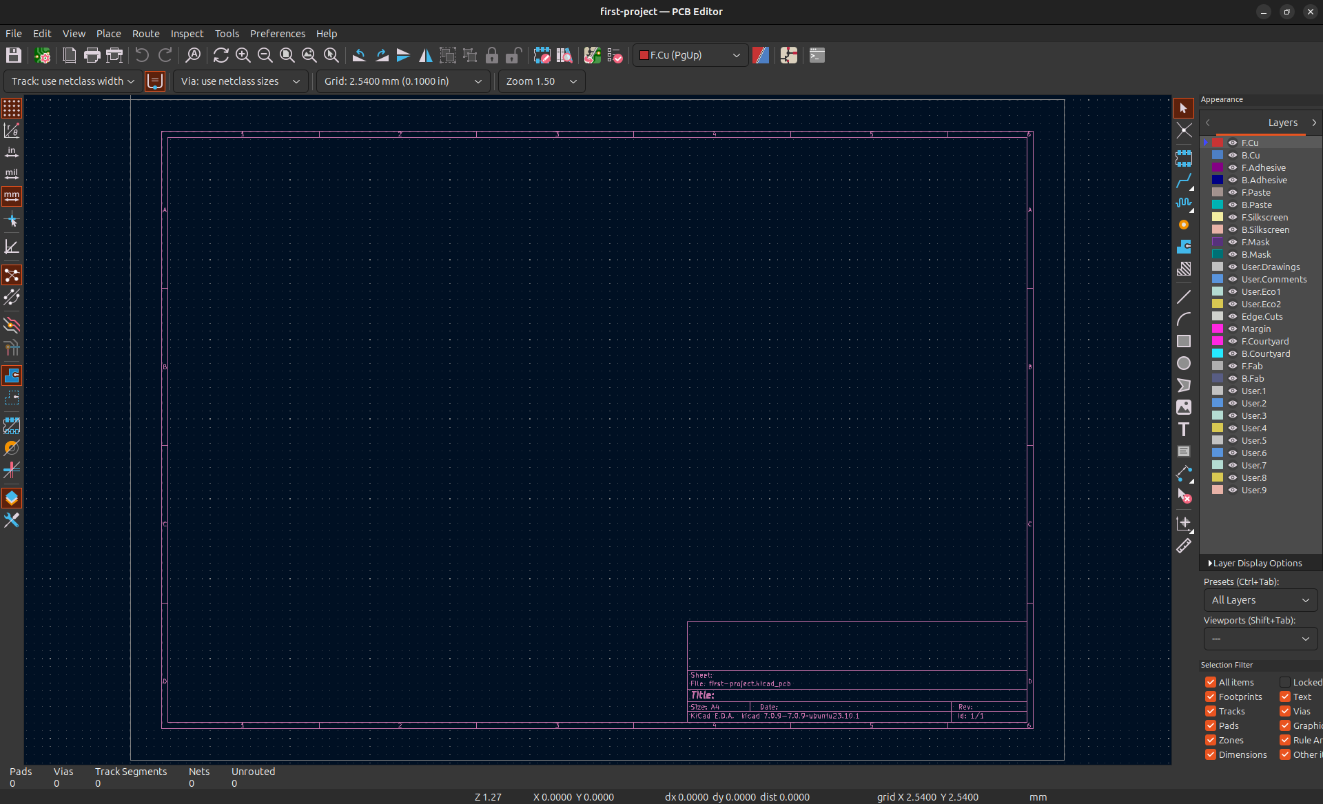
The main PCB editor window will open:
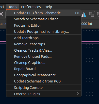
Since we already designed a schematic with footprints, we can use it by going to Tools -> Update PCB from Schematic (F8):
We’ll get a pop up telling us that it correctly processed our schematic. We just need to click Update PCB and we’ll get the option to place our components in our workplace. We’ll just put them in the top left corner for now:
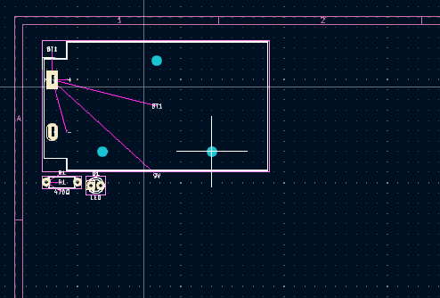
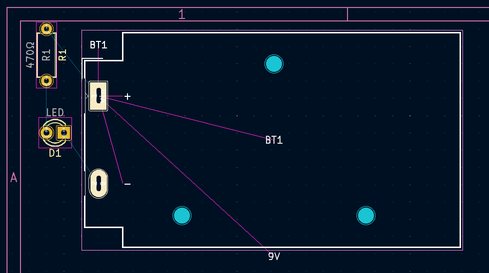
We can select and move components the same way we do it in the schematic. Just use the select tool (Esc) and drag things around. I moved the LED and resistor to the left of the battery:
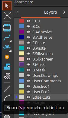
After arranging our components, we want to define the shape of our board. To do this, we need to choose the Edge Cuts layer:
Then select the Draw a line (Ctrl + Shirft + L) tool:
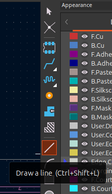
And we’ll use it to draw a rectangle around our components:
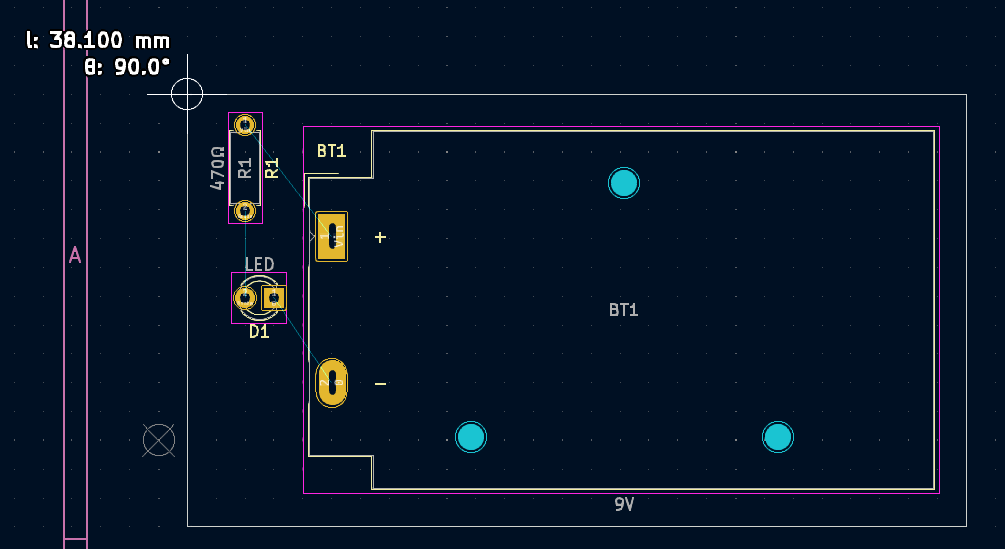
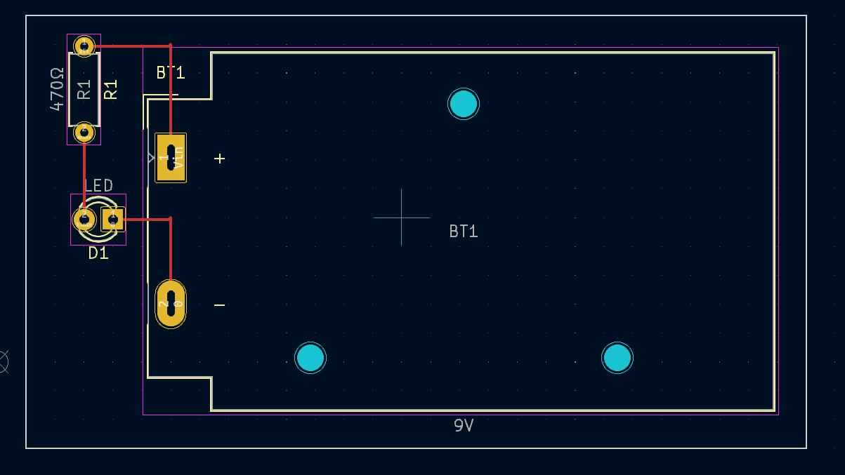
If we look closely, we will see that there are some very thin lines connecting components’ pins. These are called ratsnest and show us the connections between the components as specified in our schematic. These lines are just guides, we still have to specify how the actual copper routes will be placed on the PCB.
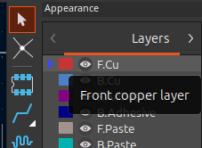
To draw our copper routes we need to first choose which copper layer to use. We’ll use the one called F.Cu:
And then choose the Route Tracks (X) tool:
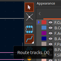
Since this is a very simple design, we can just draw our tracks following the ratsnest:
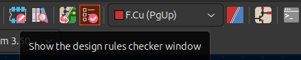
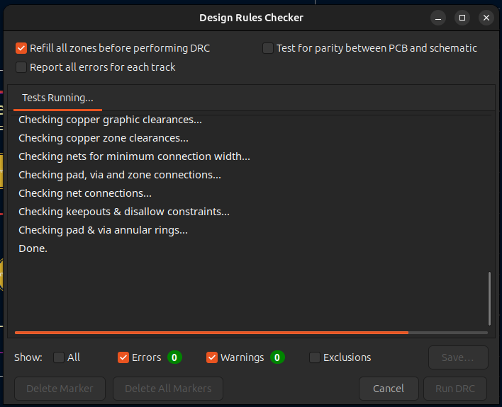
Before we call our PCB done, it’s a good idea to run PCB checks on it. For this, we need to open the design rules checker window:
After clicking Run DRC we should get 0 errors and 0 warnings:
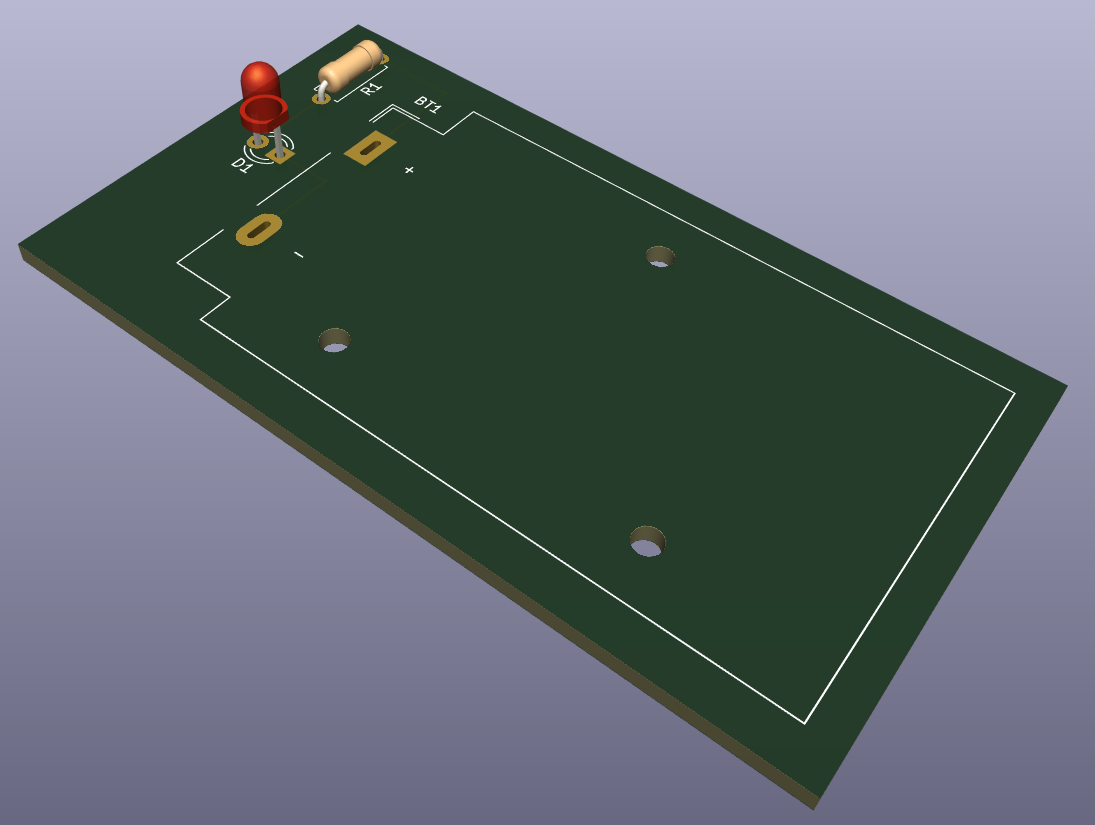
We can now consider our PCB design completed. To celebrate we can run the 3D Viewer (Alt + F3):
And admire our creation:
Conclusion
In this article we learned how to design a very simple electronics project from start to finish. We didn’t go in much dept in any particular topic, but we did a tour of the most important functions of KiCad.
If you wan to see the finished project, you can find it on github
electronics